



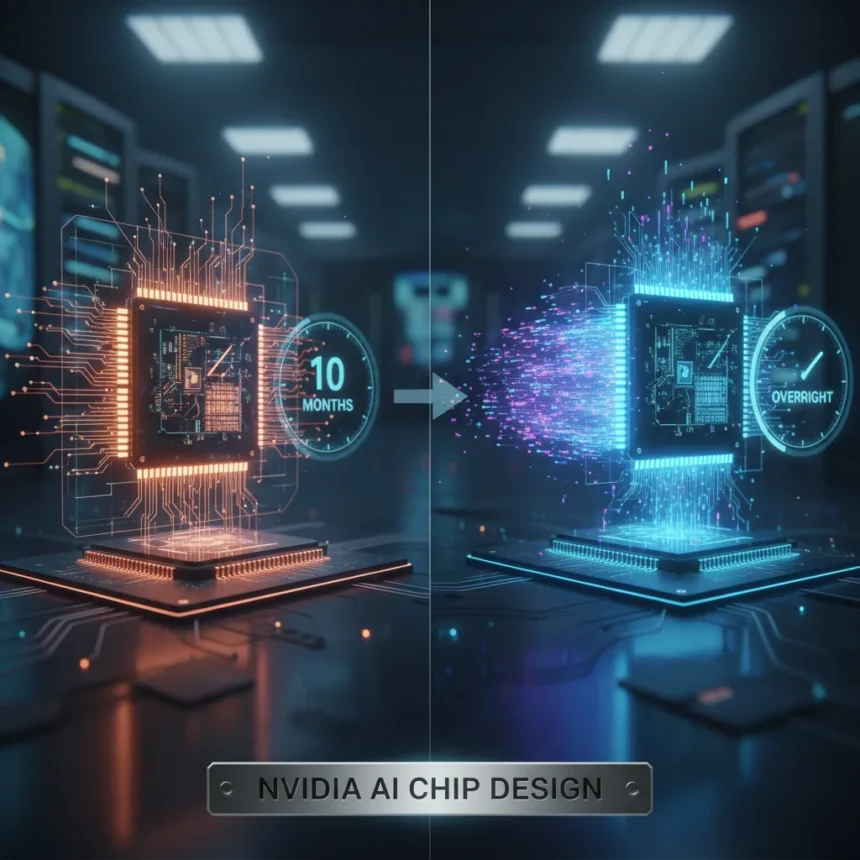
AI chip design acceleration is reshaping how semiconductor companies iterate on their most complex products. Nvidia reports that artificial intelligence has compressed a GPU design task that once consumed 10 months and eight engineers into an overnight job, yet the company acknowledges it remains a long way from fully autonomous chip design without human oversight.
Key Takeaways
- Nvidia has accelerated a specific GPU design task from 10 months with eight engineers to completion overnight using AI.
- Modern chip design involves multiple stages: requirements, circuit logic modeling, EDA software translation, microarchitecture definition, and iterative refinement.
- Full autonomous chip design is not yet feasible; human input remains essential across the design pipeline.
- Nvidia employs tens of thousands of chip design engineers, with latest processes taking a year or longer to complete.
- The semiconductor ecosystem relies on EDA tools, IP vendors, foundries, and packaging partners working in parallel.
How AI Chip Design Acceleration Works in Practice
AI chip design acceleration applies to iterative and computationally intensive stages of the design pipeline. The traditional GPU design workflow starts with high-level performance requirements, which engineers translate into an abstract circuit logic model using electronic design automation (EDA) software. From there, designers define the microarchitecture—the structural layout of logic components—and either design custom components or license intellectual property cores from vendors. Each connection between components must be specified, tested, and validated through simulation, error checking, and formal proofs.
The task Nvidia highlighted—reduced from 10 months to overnight—represents one discrete phase of this multi-stage process, not the entire chip design. This distinction matters. Accelerating a single bottleneck, even dramatically, does not mean the overall design cycle has shrunk proportionally. Nvidia still employs tens of thousands of chip design staff, and latest AI chip processes continue to span a year or longer from concept to production. The overnight acceleration is a meaningful productivity win, but it is one win in a longer race.
Why Full Autonomous AI Chip Design Remains Distant
Nvidia’s own acknowledgment that it is still a long way from AI designing chips without human input reflects the inherent complexity of semiconductor engineering. Chip design is not a single monolithic task but a constellation of interdependent decisions: balancing compute, memory, and interconnect architecture for performance, power, and area (PPA); coordinating parallel silicon, package, and software development; designing for manufacturing and test (DFM/DFT); and collaborating across an ecosystem of EDA tools, IP vendors, and foundries.


Each of these domains has its own constraints and trade-offs. An AI system that optimizes for raw performance might overlook manufacturability at a given process node. Another might maximize power efficiency at the cost of yield. Human engineers resolve these conflicts by applying domain knowledge, intuition, and business judgment—qualities that AI has not yet replicated at the scale required for autonomous design. The semiconductor industry has not produced an AI system capable of making these holistic decisions independently.
AMD faces similar timelines and complexity in its chip design operations, with tens of thousands of engineers and year-plus development cycles for advanced AI chips. The industry-wide pattern suggests that AI acceleration of specific tasks is outpacing the emergence of end-to-end autonomous design.



The Real Impact: Faster Iteration, Not Instant Chips
The practical value of AI chip design acceleration lies in enabling faster iteration cycles. When a design revision that once took weeks or months can be evaluated overnight, engineers can explore more architectural options, test more performance scenarios, and refine designs more aggressively. This speed advantage compounds over a multi-year development cycle, potentially shaving months off total timelines and allowing teams to respond more quickly to market demands or process node changes.
Nvidia co-designs its AI chips with TSMC using advanced semiconductor processes, and faster design iteration benefits both partners. The same acceleration applies to the design for manufacturing phase, where Nvidia must validate that its circuits can be reliably produced at TSMC’s foundry. Overnight simulation and validation cycles replace weeks of back-and-forth, reducing schedule risk.
What AI Cannot Yet Replace
The design process includes steps that remain fundamentally human-driven. Specifying high-level requirements—deciding what performance metrics matter most, what power budget is acceptable, what features are essential—requires business strategy and customer insight. Architects must anticipate market needs, competitive threats, and technology roadmaps. No AI system has demonstrated the ability to make these strategic choices autonomously.
Similarly, the final sign-off and risk assessment before sending designs to the fab involves experienced engineers weighing manufacturing risk, yield projections, and the cost of a failed tape-out. A single design error at an advanced process node can cost tens of millions of dollars. That responsibility remains with humans.



Is AI chip design acceleration a significant shift for the entire industry?
Not yet. While Nvidia‘s overnight acceleration of a single design task is impressive, it does not signal that autonomous chip design is imminent. The company’s own statement—that it remains a long way from full autonomy—is the most honest assessment in the industry. AI is a powerful tool for acceleration, not a replacement for chip design engineering.
How much faster is the overall chip design timeline with AI acceleration?
The research does not provide a specific overall timeline reduction. Nvidia reports one task compressed from 10 months to overnight, but chip design involves many sequential and parallel tasks. The overall impact depends on whether that task was a critical bottleneck or one of many parallel processes. Industry timelines for latest chips remain in the one-year-plus range.
Can other chip companies replicate Nvidia’s AI design acceleration?
Potentially, but with caveats. The acceleration depends on access to similar EDA tools, internal AI expertise, and large datasets of previous successful designs. Nvidia’s scale and resources give it advantages, but the underlying techniques—using AI for simulation, validation, and iterative refinement—are available to other companies with sufficient engineering depth. AMD and other semiconductor firms are pursuing similar AI-assisted design strategies.
AI chip design acceleration is real and measurable, but it is not magic. Nvidia has cracked one important bottleneck, and that matters for speed and competitiveness. What it has not done—and what remains years away—is remove the human engineer from the chip design equation. Until that changes, the semiconductor industry will continue to rely on the tens of thousands of specialists who understand both the art and science of turning silicon into the engines that power AI itself.
Edited by the All Things Geek team.
Source: Tom's Hardware