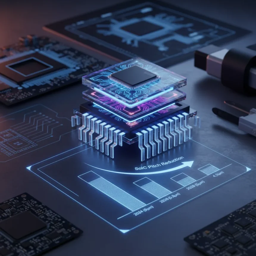
The TSMC SoIC 3D stacking roadmap represents a critical inflection point in semiconductor density. TSMC’s System-on-Integrated-Chip technology currently operates at 6-micron pitches and is charted to reach 4.5-micron pitches by 2029, compressing the interconnect spacing between stacked chiplets and unlocking new performance tiers for processor design.
Key Takeaways
- TSMC SoIC 3D stacking roadmap progresses from 6-micron to 4.5-micron pitches over five years
- Face-to-face chiplet stacking enables higher density than traditional side-by-side layouts
- Fujitsu’s Monaka CPU is among the first beneficiaries of this stacking methodology
- Tighter pitches reduce latency and power consumption between chiplet interconnects
- 3D stacking competition intensifies as Intel and other foundries pursue similar roadmaps
What the TSMC SoIC 3D stacking roadmap means for chiplet design
The roadmap signals that TSMC is betting heavily on vertical integration as the dominant architecture for next-generation processors. Chiplets stacked face-to-face—where the active sides of two dies face each other directly—allow for denser interconnects than traditional side-by-side configurations. This approach reduces the physical distance signals must travel between compute cores, memory, and I/O, cutting latency and power draw in the process.
Current 6-micron pitch technology already represents a significant step forward from earlier 3D interconnect methods. The progression toward 4.5 microns by 2029 means TSMC is targeting roughly a 25 percent reduction in pitch spacing over the roadmap window. For system designers, this translates to more aggressive chiplet density and the ability to pack more functionality into the same physical footprint.
Fujitsu’s Monaka CPU demonstrates the practical application of this trajectory. By adopting face-to-face stacking early, Fujitsu gains a competitive advantage in CPU performance per watt—a critical metric for data center and high-performance computing workloads where thermal and power constraints are non-negotiable.


How TSMC SoIC 3D stacking roadmap compares to rival approaches
Intel’s foundry roadmap includes its own 3D die stacking variant, outlined as part of the 18A process node enablement. However, TSMC’s published timeline and current production maturity at 6-micron pitches suggest TSMC has a near-term manufacturing advantage. Intel’s approach focuses on enabling 3D stacking at future nodes, whereas TSMC is already shipping designs and iterating toward tighter pitches.
Samsung and other foundries are pursuing 3D interconnect strategies as well, but none have publicly committed to a specific pitch roadmap as transparent as TSMC’s. The clarity of TSMC’s 4.5-micron target by 2029 provides design teams with a long-term planning horizon—critical for CPU architects who must commit to layouts years before production.


Why chiplet density matters now
The semiconductor industry faces a fundamental physics problem: traditional planar scaling is slowing as transistor gates approach atomic dimensions. 3D stacking sidesteps this by adding a third dimension, allowing engineers to increase die complexity and performance without shrinking transistors further. TSMC’s roadmap acknowledges this reality and positions the company to capture share in the lucrative high-performance computing segment where chiplet designs are becoming standard.
Monaka’s adoption of face-to-face stacking validates the architectural approach. As more CPU and GPU designers follow Fujitsu’s lead, demand for TSMC’s 3D interconnect capacity will grow, reinforcing TSMC’s manufacturing moat and justifying continued investment in pitch reduction.
What happens after 4.5 microns?
The roadmap extends to 2029, but TSMC’s longer-term vision likely includes further pitch compression beyond 4.5 microns. Industry sources suggest that 3-micron and sub-3-micron pitches are technically feasible, though manufacturing yields and cost economics remain open questions. TSMC’s ability to deliver on the 4.5-micron target will largely determine whether the company can sustain its foundry leadership in the 2030s.
Will my CPU use TSMC SoIC 3D stacking technology?
If you buy a high-end CPU or GPU after 2025, there is a reasonable chance it incorporates some form of chiplet stacking. Monaka is an early adopter, but major x86 and ARM designers are evaluating 3D interconnect strategies. By 2029, when 4.5-micron pitches mature, expect stacking to be commonplace in flagship processors.


How does face-to-face stacking differ from side-by-side chiplets?
Face-to-face stacking places the active surfaces of two dies directly adjacent, enabling shorter interconnect paths and higher bandwidth density. Side-by-side chiplets sit on the same substrate but are physically separated, requiring longer wires and introducing more latency. TSMC’s roadmap optimizes for face-to-face layouts, which is why the pitch reductions are so significant—tighter pitches directly translate to performance gains.
The TSMC SoIC 3D stacking roadmap is not just an engineering milestone; it is a strategic bet that 3D integration will define the next decade of processor design. Chiplet architectures are no longer a niche optimization—they are becoming the default path for performance growth. Companies that master the transition from planar to vertical designs will dominate high-performance markets. TSMC’s transparent roadmap and early leadership with Monaka suggest the company is well-positioned to lead that transition.
Edited by the All Things Geek team.
Source: Tom's Hardware