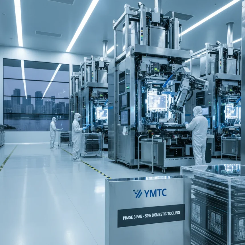
YMTC’s third Wuhan fab has cleared Beijing’s unwritten 50% domestic tooling threshold, marking the first leading-edge memory plant built to comply with China’s push for semiconductor self-sufficiency. The YMTC domestic tooling threshold achievement positions Yangtze Memory Technologies, China’s largest NAND flash memory chipmaker founded in 2016, to accelerate its shift toward advanced 3D NAND production while navigating intensifying US export restrictions on chipmaking equipment.
Key Takeaways
- YMTC’s Phase 3 fab sources over 50% of equipment and materials from domestic Chinese suppliers, meeting Beijing’s domestic tooling requirement.
- Phase 3 construction is complete with equipment installation underway; operations expected to begin late 2025, reaching 50,000 wafers per month by 2027.
- YMTC currently operates two Wuhan fabs producing 200,000 wafers monthly combined; Phase 3 will add 50,000 wpm capacity.
- Two additional fabs planned beyond Phase 3, each with 100,000 wpm capacity, potentially tripling total output to 600,000 wpm.
- Phase 3 allocates roughly 50% of capacity to DRAM production alongside NAND, with development of through-silicon via packaging for AI accelerator memory.
How YMTC’s Domestic Tooling Threshold Shifts China’s Chip Strategy
The YMTC domestic tooling threshold compliance represents a watershed moment for Chinese semiconductor independence. Rather than relying on foreign equipment suppliers like ASML or Applied Materials for critical vertical stacking tools, Phase 3 sources the majority of its manufacturing equipment and materials from domestic Chinese companies. This architectural shift allows YMTC to operate independently of US export controls that have strangled Chinese chipmakers since 2022.
The timing is critical. US politicians proposed additional restrictions on chipmaking tool exports this month, targeting remaining loopholes that allow advanced equipment sales to Chinese fabs. By meeting the domestic tooling threshold now, YMTC insulates itself from future sanctions while demonstrating that Chinese suppliers can manufacture competitive equipment for leading-edge memory production. The company’s Xtacking 4.0 architecture already matches products from sector leaders like Samsung Electronics, proving domestic tools need not mean inferior performance.
YMTC’s current two-fab operation in Wuhan produces a combined 200,000 wafers per month. Phase 3 will add 50,000 wpm capacity by 2027, but the real expansion lies ahead: two additional fabs are planned, each with full 100,000 wpm capacity. If realized, this expansion would lift total output to 600,000 wpm across five Wuhan facilities—more than tripling current production and positioning YMTC as a genuine rival to Samsung and SK Hynix in global memory markets.


3D NAND and Wafer Bonding: Where YMTC’s Strengths Lie
The Phase 3 fab’s design reflects YMTC’s strategic pivot toward 3D NAND production, where the company’s wafer bonding expertise provides a competitive edge. Rather than stacking memory layers using traditional deep trench isolation, YMTC’s approach leverages horizontal bonding of pre-fabricated wafers—a technique that reduces defects and simplifies manufacturing at extreme layer counts. This architectural advantage becomes increasingly valuable as competitors push toward 200+ layer NAND stacks.
Phase 3 allocates approximately 50% of its capacity to DRAM production rather than NAND, diversifying YMTC’s product portfolio. The company is simultaneously developing through-silicon via (TSV) packaging for high-bandwidth memory used in AI accelerators, signaling ambitions beyond traditional storage chips. This dual focus hedges against commodity NAND price swings while capturing higher-margin AI memory demand.


The domestic tooling threshold compliance is not merely a regulatory checkbox—it enables YMTC to customize equipment for its bonding-centric architecture without waiting for foreign tool vendors to adapt their designs. Chinese equipment makers can iterate rapidly, tailoring machines specifically for YMTC’s process flows. This feedback loop accelerates innovation in ways that traditional vendor relationships, constrained by export rules, cannot match.
Expansion Plans and the Geopolitical Calculus
YMTC’s announcement of two additional 100,000 wpm fabs signals confidence in sustained demand despite US pressure. Each new fab will presumably follow Phase 3’s domestic tooling model, embedding Chinese equipment suppliers deeper into YMTC’s supply chain. This strategy reduces exposure to future US export restrictions while creating a domestic ecosystem that other Chinese chipmakers can tap into.
The expansion occurs against a backdrop of escalating US-Sino trade tensions. Unlike TSMC or Samsung, which depend on US equipment vendors like ASML for extreme ultraviolet lithography, YMTC is architecting itself around domestic alternatives. While Chinese EUV tools lag Western equivalents, YMTC’s 3D NAND strategy requires fewer of them—the company can achieve layer counts through vertical bonding rather than pushing lithography to absolute limits. This architectural choice, born from necessity, may paradoxically prove more resilient than competitors’ approaches.
Is YMTC’s domestic tooling strategy sustainable long-term?
YMTC’s reliance on domestic equipment will face real technical hurdles as process nodes shrink. Chinese tool makers lack the decades of R&D investment embedded in Western suppliers, and certain specialized equipment—such as advanced inspection systems—remain difficult to replicate. However, for 3D NAND production, where YMTC’s bonding architecture reduces dependence on extreme lithography, the domestic tooling model appears viable. The company is betting that architectural innovation can substitute for incremental equipment superiority.


How much capacity will YMTC add with the two new fabs?
The two additional fabs planned beyond Phase 3 will each reach 100,000 wafers per month capacity, adding 200,000 wpm combined. Combined with Phase 3’s 50,000 wpm, YMTC’s total output would reach 450,000 wpm across three new fabs, plus the existing 200,000 wpm from current operations—totaling 650,000 wpm across five Wuhan facilities.
When will Phase 3 begin production?
Phase 3 construction is complete with equipment installation currently underway. Operations are expected to commence in late 2025, with the fab reaching full 50,000 wpm capacity by 2027. The gradual ramp-up reflects typical fab commissioning timelines, where yield optimization and process refinement require months of production runs.
YMTC’s Phase 3 fab represents a pivotal moment for Chinese semiconductor self-sufficiency. By meeting the domestic tooling threshold, the company has proven that advanced memory production need not depend on Western suppliers—a lesson that will reverberate through Beijing’s industrial policy for years. The planned expansion to 600,000 wpm suggests YMTC believes this model works, and competitors will inevitably follow. For the US, the shift underscores how export restrictions, rather than halting Chinese progress, accelerate the very ecosystem independence they aim to prevent.
Edited by the All Things Geek team.
Source: Tom's Hardware