


Huawei’s Tau Scaling Law represents a fundamental shift in how the semiconductor industry measures progress. Rather than chasing ever-smaller transistors, the Tau Scaling Law proposes replacing geometric scaling with time (τ) scaling as the guiding principle for semiconductors and electronic systems. This matters now because Moore’s Law—the 50-year-old rule that transistor counts double roughly every two years—has hit severe physical limits and diminishing economic returns, and Huawei is betting its competitive future on a credible alternative.
Key Takeaways
- Huawei introduced the Tau Scaling Law at the 2026 IEEE ISCAS conference, shifting focus from transistor size to signal propagation delay.
- LogicFolding architecture breaks traditional circuit boundaries to reduce wiring delays and improve transistor density.
- First Kirin chips using LogicFolding are scheduled for Fall 2026.
- Huawei projects 14 Å (1.4 nm)-equivalent transistor density by 2031 using this framework.
- The approach spans optimization across device, circuit, chip, and system levels.
What the Tau Scaling Law actually does
The Tau Scaling Law redefines performance evolution by treating signal delay—not transistor size—as the primary metric for progress. According to Huawei, the framework optimizes across four distinct layers: devices, circuits, chips, and systems. At the device level, engineers focus on minimizing resistance and parasitic capacitance in transistors and interconnects. At the circuit level, a new technology called LogicFolding breaks traditional layout boundaries and shortens critical-path wiring. This is where the architecture diverges sharply from conventional chip design, which has relied on shrinking features to improve performance. Instead, Huawei is rearranging how logic flows through silicon to reduce the time signals take to traverse circuits.
The comparison to Moore’s Law is instructive. Moore’s Law treated the production line as fixed and added more workers—shrinking transistors to pack more onto a die. The Tau Scaling Law, by contrast, speeds up the turnover of parts on that line—optimizing how data and instructions flow through the system. This shift matters because advanced lithography nodes (the smallest transistor sizes) are becoming prohibitively expensive and physically constrained. Huawei’s approach suggests you do not need latest fab processes to achieve significant performance gains if you optimize the entire stack simultaneously.
How LogicFolding changes chip architecture
LogicFolding is the centerpiece technology under the Tau framework. The architecture expands from single-layer to double-layer logic design, allowing circuits to operate more efficiently without relying exclusively on leading-edge lithography. At the chip level, Huawei combines software, architecture, and silicon in a coordinated design that controls instruction and data flows in a workload-driven way. This full-stack approach reduces end-to-end execution time by eliminating unnecessary detours in how data moves through the system.


At the system level, Huawei has developed UnifiedBus, which redefines interconnect protocols for computing systems and enables unified memory addressing and native memory semantics for SuperPoDs. In practical terms, this means reducing the latency penalties that typically occur when different components communicate. The multi-level co-optimization mechanism spans from individual transistors up to entire computing clusters, creating a unified optimization surface that conventional architectures lack.
Tau Scaling Law vs. traditional semiconductor progress
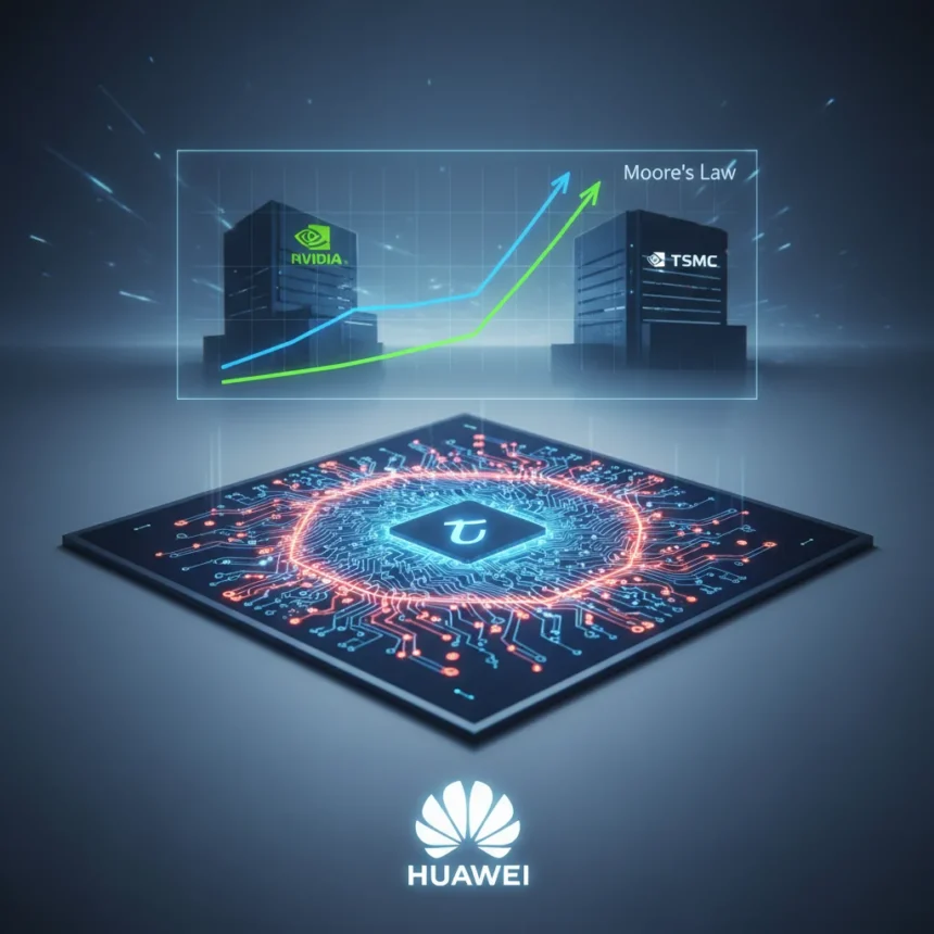
The semiconductor industry has relied on Moore’s Law as a north star for five decades. Nvidia and TSMC have built their dominance on mastering advanced process nodes—the race to smaller, faster transistors. Huawei’s Tau Scaling Law challenges this paradigm directly. Where Nvidia focuses on maximizing performance within a given lithography node, Huawei is arguing that optimizing time-constant compression across all layers can deliver comparable or superior results without the cost and complexity of ultra-advanced fabrication.



This is not to say Huawei is abandoning process technology. Rather, the company is proposing that process scaling and system innovation operate on equal footing. Huawei projects that high-end chips based on the Tau Scaling Law will reach transistor density equivalent to 14 Å (1.4 nm) processes by 2031, and that hardware integration could increase more than 100 times by 2035. These are forward-looking projections, not verified results. But they signal that Huawei sees a path to competitive parity without waiting for TSMC’s most advanced nodes.
When will Tau Scaling arrive in commercial chips?
Huawei has committed to real-world validation. The company says Kirin chips scheduled to launch in Fall 2026 will be the first ever to adopt the LogicFolding architecture and will considerably enhance performance. This timeline is crucial—it moves the Tau Scaling Law from academic presentation to market test. If Kirin chips deliver on the performance claims, other chipmakers will face pressure to adopt similar optimization strategies. If they underperform, the framework’s credibility will suffer immediately.
The announcement at the 2026 IEEE International Symposium on Circuits and Systems positioned the Tau Scaling Law as a post-Moore’s Law alternative at a moment when the industry lacks a widely accepted replacement framework. This is both Huawei’s opportunity and its risk. Positioning a new architecture as the future of semiconductors is bold. Delivering on that promise in a highly competitive market is another matter entirely.
Is Tau Scaling Law a credible alternative to Moore’s Law?
The Tau Scaling Law addresses a genuine problem. Moore’s Law has become increasingly expensive to sustain, and further process scaling faces quantum mechanical barriers. Huawei’s shift toward time-delay optimization and multi-layer co-design is theoretically sound—signal propagation delay is indeed a bottleneck that conventional designs do not systematically address. However, the framework’s success depends on whether it can be implemented consistently across diverse workloads and whether other chipmakers can adopt or replicate the approach.



Huawei’s claims of feasibility, universality, and sustainability are company assertions at this stage. The projected 14 Å-equivalent density by 2031 and 100x integration gains by 2035 are forward-looking statements, not independently verified outcomes. The real test arrives in Fall 2026 when Kirin chips hit the market. Until then, the Tau Scaling Law remains a compelling alternative framework rather than a proven replacement for Moore’s Law.
What does this mean for the semiconductor industry?
If Huawei’s Tau Scaling Law gains traction, it could reshape how chipmakers approach design. The framework suggests that performance improvements do not require constant access to the absolute cutting edge of lithography. This has implications for companies without TSMC or Samsung partnerships, and it could democratize advanced chip design by shifting emphasis from process node to architectural optimization. Conversely, if the approach proves niche or limited to Huawei’s specific use cases, it may remain a footnote in semiconductor history rather than a paradigm shift.
Will Tau Scaling Law help Huawei catch Nvidia and TSMC?
Huawei’s stated goal is to close the gap with Nvidia and TSMC. Nvidia dominates AI accelerators through architectural innovation and manufacturing partnership with TSMC. TSMC controls the process technology that enables that dominance. Huawei cannot easily replicate either advantage. The Tau Scaling Law is an attempt to sidestep the process-node race entirely—to compete on architectural and system-level efficiency rather than fab leadership. Whether this strategy works depends on whether time-delay optimization delivers real-world performance gains that matter to Huawei’s target markets. Fall 2026 will provide the first concrete evidence.
Can other chipmakers adopt the Tau Scaling Law?
The framework is presented as universal and feasible, but adoption by other companies is unclear. Nvidia and TSMC have deep investments in conventional scaling. Intel, AMD, and others have their own architectural roadmaps. Huawei has not announced licensing or partnerships that would allow other chipmakers to implement LogicFolding. If the technology remains proprietary to Huawei, its industry-wide impact will be limited, regardless of its technical merit.
What happens if Moore’s Law truly ends?
The semiconductor industry has operated under Moore’s Law for so long that alternative frameworks feel abstract. But the physical and economic constraints are real. If transistor scaling slows or stops, the industry must find new sources of performance gain. The Tau Scaling Law is one proposal. Other approaches—chiplets, 3D stacking, domain-specific architectures—exist alongside it. The future likely involves multiple paths rather than a single successor to Moore’s Law. Huawei’s contribution is a credible alternative that shifts optimization from geometry to time, backed by a commitment to commercial validation in 2026.
The Tau Scaling Law matters because it challenges the assumption that semiconductor progress is inseparable from lithography advancement. If Huawei’s Fall 2026 Kirin chips deliver meaningful performance gains through LogicFolding architecture, the framework gains legitimacy as a post-Moore’s Law path. If they underperform, the industry will continue searching for alternatives. Either way, the days of relying solely on transistor shrinkage to drive progress are ending. Huawei is betting that optimizing time-constant compression across all layers offers a viable next chapter.
Edited by the All Things Geek team.
Source: TechRadar