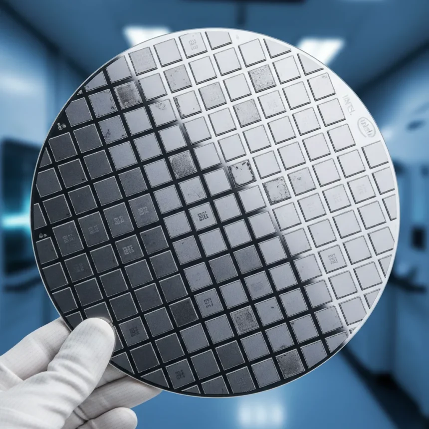
Wafer yield variability refers to inconsistent chip production across individual wafers, where some yield far more usable dies than others. Intel is now systematically reducing this variability, particularly at wafer edges, to extract more revenue from each production run. The effort ties directly to the company’s 18A process node ramp, where early manufacturing volatility has created both supply constraints and optimization opportunities.
Key Takeaways
- Intel is minimizing wafer-to-wafer yield volatility to increase sellable CPUs per wafer and boost revenue.
- 18A process shows steady yield progression in 2026, expected to reach industry standard levels by 2027.
- RibbonFET transistors and PowerVia backside power delivery introduce early-stage variability but drive efficiency gains.
- AI-powered yield analysis tools achieve over 90% accuracy in detecting defects and abnormalities across entire wafer lots.
- Intel 18A density stands at 238 million transistors per square millimeter, lower than TSMC N2 but stronger in performance per watt.
How Intel Is Tackling Wafer Yield Variability
The core problem is straightforward: some wafers produce significantly more usable chips than others. Intel CFO David Zinsner acknowledged this volatility directly, noting that “there is a lot of volatility, some wafers are yielding a lot less and some are yielding a lot more”. This unpredictability undermines manufacturing efficiency and revenue predictability. Under CEO Tan Chie Hao, Intel has prioritized minimizing this wafer-to-wafer variance, and early results suggest the strategy is working. Zinsner stated the company expects “a pretty steady yield progression as we go through this year, probably a bit ahead of schedule”.
The 18A process node introduced two major architectural changes—RibbonFET gate-all-around transistors and PowerVia backside power delivery—that contributed to initial yield unpredictability. These novel technologies create manufacturing complexity that older processes do not face. However, Intel’s ability to reduce variability as production ramps suggests the company is learning to control these new process steps more precisely.
AI and Machine Learning Drive Yield Optimization
Intel has deployed AI-driven yield analysis tools to identify and root-cause defects at scale. The system achieves “greater than 90 percent accuracy in baseline pattern recognition” and can “identify multiple gross functional abnormalities per wafer”. Rather than sampling wafers for inspection, Intel now examines 100% of wafers per lot, catching problems early and preventing affected dies from reaching customers.


Beyond defect detection, Intel uses deep generative diffusion models to predict electrical test metrics post-manufacture, incorporating SPICE parameters to optimize designs at the stage before physical production. This approach allows engineers to anticipate yield challenges before wafers even reach the fab, reducing costly rework and scrap. The combination of automated inspection and predictive modeling creates a feedback loop that continuously tightens yield control.
What Wafer Yield Variability Means for 18A Revenue
Reducing wafer yield variability directly translates to revenue per wafer. If a wafer typically produces 100 usable dies but variability causes some wafers to yield only 60 dies while others yield 140, the average is 100—but the unpredictability creates supply gaps and forces Intel to hold excess inventory. By flattening the distribution, Intel ensures more wafers cluster near the higher end, increasing the floor of usable chips per production run. This matters especially at wafer edges, where process variation has historically been most severe. Extracting more sellable CPUs from edge regions alone can meaningfully improve yield economics.


The 18A process is expected to reach industry-standard yield levels by 2027, but Intel’s trajectory suggests it will arrive ahead of that target. Early production of Panther Lake CPU tiles began in late 2025 at Oregon, with high-volume manufacturing ramping at Fab 32 in Arizona. Each quarter of improved yields in 2026 directly increases the revenue generated per wafer, a critical metric for foundry economics and internal product supply.
PowerVia Boosts Efficiency While Adding Manufacturing Complexity
PowerVia backside power delivery separates power distribution from the wafer’s front side, reducing resistance and voltage droop. The technology improves standard cell utilization by 5-10% and boosts ISO power performance by up to 4%. These gains are significant for power-constrained AI chips, where efficiency directly impacts total cost of ownership. However, backside power delivery is a relatively new technique in high-volume manufacturing, and Intel’s ability to minimize variability while implementing it demonstrates process maturity.
Compared to TSMC’s N2 process, Intel’s 18A achieves higher performance per watt despite lower transistor density. TSMC N2 reaches 313 million transistors per square millimeter, while Intel 18A stands at 238 MTr/mm². For compact mobile or edge devices, TSMC’s density advantage matters. For AI accelerators and server CPUs where power efficiency and performance dominate cost considerations, Intel’s per-watt advantage is the more relevant metric.
Why Yield Variability Matters Now
AI demand has created a supply crunch for advanced process nodes. Every wafer that yields fewer usable chips represents lost revenue and delayed customer shipments. Intel’s focus on reducing variability is not a long-term optimization—it is an immediate competitive necessity. Competitors like TSMC have spent decades perfecting yield control; Intel is playing catch-up on a new process node while ramping production at scale. Success here determines whether 18A becomes a viable external foundry offering or remains constrained to internal use.


Is Intel ahead of schedule on 18A yields?
Intel CFO David Zinsner stated the company expects “pretty steady yield progression” through 2026, “probably a bit ahead of schedule” compared to the 2027 target for industry-standard yields. However, these are company statements, not independent verification. Actual yield metrics remain proprietary, and early-stage HVM variability is typical for new process nodes.
How does PowerVia improve performance compared to traditional power delivery?
PowerVia reduces voltage droop and resistance by moving power distribution to the wafer’s back side. This enables 5-10% better standard cell utilization and up to 4% improvement in ISO power performance, translating to lower power consumption at equivalent performance levels.
What is the difference between Intel 18A and TSMC N2 density?
TSMC N2 achieves 313 million transistors per square millimeter, while Intel 18A reaches 238 MTr/mm². TSMC’s higher density suits compact devices; Intel’s architecture prioritizes performance and efficiency per watt for power-intensive workloads like AI inference and training.
Intel’s push to reduce wafer yield variability reflects a company racing to prove 18A viability in a market where every usable chip matters. The combination of novel transistor architectures, backside power delivery, and AI-driven yield optimization positions Intel to extract more revenue from each wafer—if the company can sustain the yield progression it has promised. The next 12 months will reveal whether Intel’s trajectory holds or whether the complexity of 18A manufacturing proves harder to control than early statements suggest.
Edited by the All Things Geek team.
Source: Tom's Hardware