Clay PCBs prehistoric firing represents a radical rejection of industrial electronics manufacturing. Patrícia J. Reis and Stefanie Wuschitz of Feminist Hackerspaces have published a complete guide to creating functional circuit boards from local clay, 3D-printed stamps, waste silver paint, and components salvaged from broken electronics—all fired using prehistoric open-fire techniques.
Key Takeaways
- Working electronics can be made from clay fired in open wood fires using 18th-century pottery techniques.
- Silver paint from jewelry factory waste remains conductive and solderable after firing; other metals tested failed.
- Components are urban-mined from discarded Arduino boards and desoldered junk electronics.
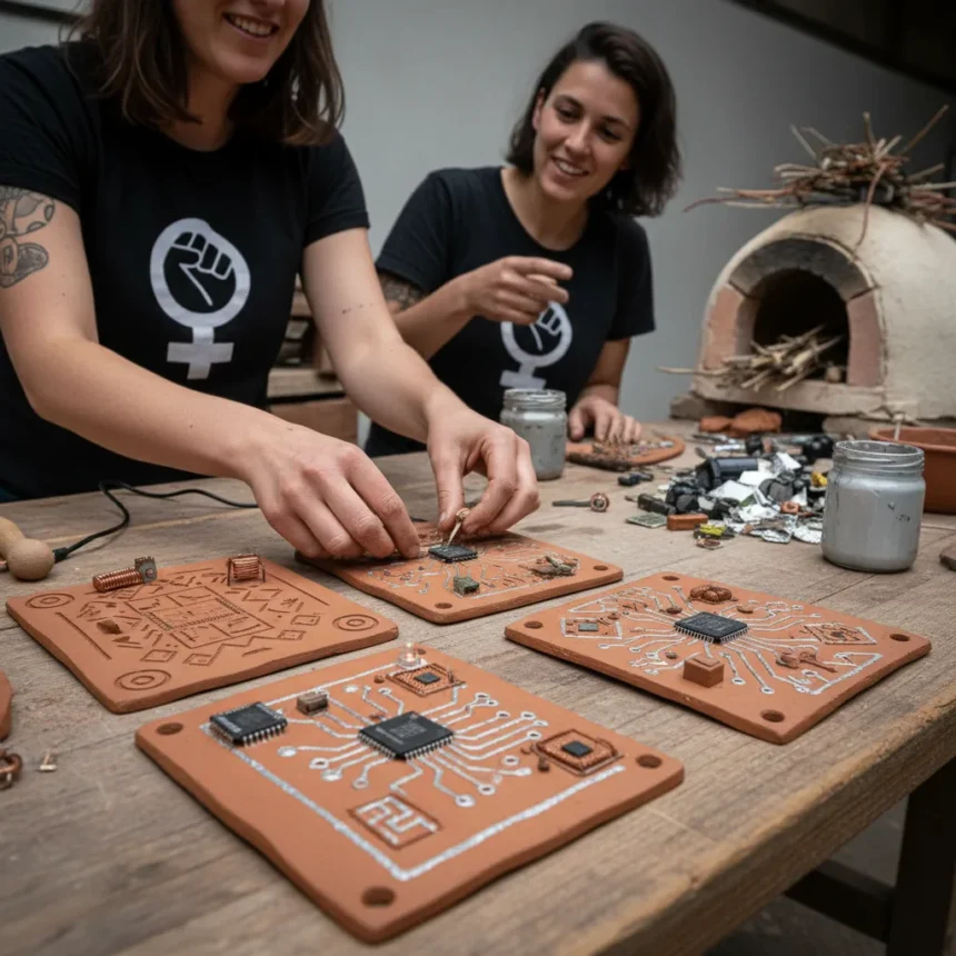
- Clay flattened to 1 cm thickness and embossed with 3D-printed circuit stamps before firing.
- The process claims zero-impact potential when clay is collected mindfully from local sources.
Why Clay PCBs Matter Now
Electronics waste is a crisis. Global supply chains for printed circuit boards depend on toxic chemical etching, hazardous materials, and extraction-heavy manufacturing. Clay PCBs prehistoric firing offers an alternative that challenges the assumption that modern electronics require industrial infrastructure. The tutorial is both artistic provocation and functional proof-of-concept—working demo boards blink and function, proving the concept is not theoretical.
This matters because it exposes how much of electronics manufacturing is convention rather than necessity. If you can solder components to silver traces burned into clay, the entire narrative around PCB economies shifts. It is not about replacing industrial production; it is about proving that alternatives exist and that extreme DIY remains possible.
The Step-by-Step Process for Clay PCBs Prehistoric Firing
The workflow begins with clay collection. Identify and source local wild clay with awareness of soil qualities, collecting only small quantities to minimize environmental impact. Sieve the raw soil to remove debris and prepare it for shaping. Flatten the clay to approximately 1 cm thickness using a dough roller and wooden slats—the material is fragile and prone to edge splitting, but cracks outside the circuit area are acceptable.


Next, emboss circuit traces into the flattened clay using a 3D-printed stamp. The stamp pattern becomes the pathway for conductivity. Fill the embossed traces with silver paint sourced from jewelry factory waste dust—this is the critical material choice. Silver remains conductive and solderable after firing, while other metals tested did not survive the high-temperature process.
Firing uses prehistoric open-fire technique learned from Heinz Lackinger, a pottery craftsman in Donnerskirchen, Austria, who uses an 18th-century ground-hole method. Dig or reuse a backyard ground hole. Start a normal fire with dry forest branches for initial heat and drying, placing clay boards around the fire perimeter. Build a base layer of thicker sticks under the boards, then stack thinner branches on top. The entire process relies on wood fire alone—no kilns, no electricity, no industrial equipment.


After firing cools completely, solder urban-mined components to the silver traces. ATmega328 microcontrollers salvaged from broken Arduino boards work reliably. Other components—resistors, capacitors, LEDs—are desoldered from junk electronics. The final boards function as working electronics, capable of blinking LEDs or running simple code.
Materials and Sourcing for Clay PCBs Prehistoric Firing
The entire material list can be sourced locally or from waste streams. Clay comes from your own soil. The 3D-printed stamp can be designed and printed with any standard 3D printer. Silver paint is the constraint—it must come from jewelry factory waste dust to maintain the zero-impact philosophy, though this requires a local supplier relationship.
Components are urban-mined: ATmega328s from defunct Arduino boards, passive components from broken electronics, LEDs from old gadgets. This approach turns electronic waste into feedstock rather than landfill. The philosophy is not just environmental; it is about rejecting the idea that new electronics require new materials extracted from the earth.
Compared to traditional toner-transfer PCB methods, which rely on commercial chemicals and laser printers, clay PCBs prehistoric firing appears primitive by design. But that primitiveness is the point. Toner transfer still requires industrial supplies. Clay firing requires only local materials and fire. The trade-off is fragility and lower component density, but for simple circuits—blinky boards, sensor nodes, educational projects—the limitations are acceptable.


Environmental and Ethical Claims
The creators claim the process can achieve 100% fair trade and zero-impact electronics if clay is collected mindfully in small quantities from local sources. This is aspirational language worth scrutinizing. Silver paint still requires industrial waste sourcing and purchasing, so it is not truly zero-impact. The claim is better understood as zero-impact clay sourcing and minimal-impact component reuse, with an asterisk on the silver paint.
What is genuine is the reduction in chemical pollution compared to industrial PCB etching, the reuse of salvaged components instead of virgin manufacturing, and the elimination of industrial infrastructure from the fabrication process. A clay board fired in a backyard fire produces less environmental harm than a board etched with ferric chloride or produced in a factory running thousands of kilowatts of power.
The project is positioned as half art, half extreme DIY, half environmental consciousness—which adds up to more than 100%, reflecting its hybrid nature. It is not a scalable replacement for industrial PCBs. It is a statement that electronics manufacturing can be radically decentralized and that the current supply chain is a choice, not an inevitability.
Accessibility and Learning
The tutorial is freely shared online and designed for accessibility. Feminist Hackerspaces emphasizes that anyone with access to clay, a 3D printer, waste silver paint, and a fire can attempt this. The learning curve is steep—firing clay is unforgiving, and soldering requires skill—but the barrier is knowledge and practice, not capital or industrial access.
The portable lab-in-a-backpack concept is central to the philosophy: dirt-to-blinky electronics in the woods, with minimal equipment. This appeals to artists, educators, and hackers interested in alternative manufacturing. It also appeals to people in regions without reliable access to commercial PCB services, though the guide does not explicitly market itself that way.
Is clay PCB firing actually reliable?
Yes, working demos have been confirmed to blink and function. The silver traces remain conductive after firing, and components solder reliably. The boards are fragile and less elastic than industrial PCBs, but for low-power applications and educational use, they work. Reliability is not industrial-grade, but it is sufficient for proof-of-concept and artistic projects.
Can you use other metals instead of silver paint?
The brief does not detail which metals were tested or why they failed, only that silver succeeded and other metals did not survive the firing process. Silver is the only confirmed conductive option post-firing. Experimenting with alternatives is possible but not documented in the tutorial.
Where do you source silver paint from jewelry factory waste?
The guide recommends finding a local jewelry factory or supplier and requesting waste dust. This requires local sourcing and relationship-building rather than mail-order purchasing. The specificity varies by region; readers in areas without jewelry manufacturing may need to be creative or substitute with commercially available metallic paint (though conductivity post-firing is unverified).
Clay PCBs prehistoric firing is not a solution to electronics waste at scale, but it is a powerful proof that the industrial PCB economy is not inevitable. It demonstrates that working electronics can emerge from local clay, salvaged components, and fire—challenging assumptions about what manufacturing requires and who gets to participate in it. For hackers, artists, and educators willing to embrace fragility and embrace fire, it opens a path to electronics that bypasses industrial supply chains entirely.
Edited by the All Things Geek team.
Source: Tom's Hardware