TSMC’s process technology roadmap through 2029 marks a strategic departure from traditional unified development, splitting its advanced node strategy into two distinct tracks: one optimized for client applications and another for high-performance data center processors. This bifurcated approach fundamentally reshapes how the world’s largest chipmaker will compete over the next five years, with major implications for Apple, Intel, AMD, and the broader semiconductor industry.
Key Takeaways
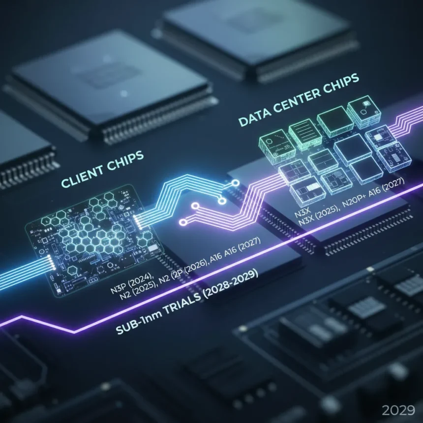
- TSMC splits roadmap into client-focused nodes (A14, A13, N2U) and data center nodes (A16, A12, N2X) through 2029.
- A16 production delayed to 2027, moving away from annual node cadence.
- A14 (1.4nm) targets mass production in 2028 with up to 30% performance and efficiency gains.
- Sub-1nm process trials begin in 2029 at 5,000 wafers per month across Taiwan facilities.
- TSMC maintains 2-3 year technological lead over Samsung and Intel in process nodes.
TSMC Process Technology Roadmap Separates Client and Data Center Strategies
The bifurcated approach splits TSMC’s advanced roadmap into two parallel tracks optimized for different market demands. Client applications—iPhones, MacBooks, and mainstream processors—will follow the A14, A13, and N2U nodes, while high-performance data center chips destined for cloud computing and AI infrastructure will pursue A16, A12, and N2X nodes. This divergence reflects the reality that mobile and desktop processors prioritize power efficiency and per-core performance, while data center chips demand maximum throughput and density.
The separation also signals TSMC’s confidence in maintaining distinct competitive advantages across multiple segments simultaneously. Rather than forcing a single node to serve all markets, the company can optimize each path independently. Client nodes can emphasize battery life and thermal efficiency, while data center nodes can prioritize raw compute density and interconnect bandwidth. This flexibility is a structural advantage over competitors pursuing monolithic roadmaps.
A16 Slips to 2027, Breaking TSMC’s Annual Cadence
The delay of A16 production to 2027 represents a notable shift in TSMC’s historical pace. For years, the company maintained roughly annual process node releases, but this roadmap shows the company is willing to extend timelines when engineering challenges demand it. The A16 node, designated for data center applications, likely faces greater technical hurdles than previous generations, particularly in achieving the density and power characteristics required for server-class chips.

This slowdown does not signal weakness. Instead, it reflects TSMC’s pragmatic engineering approach: shipping a mature, reliable node on time matters more than hitting an arbitrary calendar deadline. A16 arriving in 2027 gives the company three years to perfect the technology before mass production, reducing the risk of early-stage defects or yield problems that could damage customer relationships.
A14 Aims for 2028 Mass Production With Significant Efficiency Gains
The A14 node (1.4nm) is slated for mass production in 2028, with TSMC targeting up to 30% performance and efficiency improvements over preceding generations. This figure is substantial—a 30% efficiency gain translates directly to longer battery life for mobile devices or lower power consumption for data center workloads. For Apple, which will likely be the first customer for A14 in client applications, this means iPhones and Macs could see meaningful jumps in processing power without sacrificing battery endurance.


The 2028 timeline gives TSMC approximately three years from the current roadmap announcement to refine A14 for high-volume manufacturing. This extended development window reduces the risk of yield problems or reliability issues that plagued earlier advanced nodes at other foundries. TSMC’s track record suggests the company will deliver on this promise, maintaining its 2-3 year lead over Samsung and Intel in process maturity.
Sub-1nm Trials in 2029 Position TSMC for the Decade Ahead
The most ambitious element of the roadmap is sub-1nm process trials beginning in 2029 at 5,000 wafers per month, utilizing the A10 facility in Tainan, Taiwan, across multiple production lines. Sub-1nm represents the next frontier in Moore’s Law, a milestone that will define semiconductor leadership throughout the 2030s. TSMC’s willingness to commit to trial production by 2029 suggests the company believes it can overcome the fundamental physics challenges that have slowed progress at smaller dimensions.
Apple is expected to be the primary customer for sub-1nm trials, potentially receiving the first sub-1nm chips for iPhone and Mac processors in the late 2020s. This advantage secures Apple’s position as the world’s most advanced chip consumer and reinforces TSMC’s role as the indispensable partner for the world’s most valuable technology companies. No other foundry—Samsung, Intel, or emerging competitors—has announced comparable sub-1nm timelines.
How Does TSMC’s Roadmap Compare to Competitors?
TSMC maintains a structural 2-3 year lead over Samsung and Intel in process technology maturity. Samsung’s foundry division has struggled with yield and reliability issues at advanced nodes, while Intel is rebuilding its foundry business from a weaker starting position. Neither competitor has announced sub-1nm trials for 2029. This gap ensures that TSMC will remain the exclusive supplier of the world’s most advanced chips for years to come, a position that translates directly into pricing power and customer lock-in.


The bifurcated strategy also differentiates TSMC from competitors pursuing unified roadmaps. By optimizing separate tracks for client and data center applications, TSMC can deliver tailored solutions that monolithic approaches cannot match. This architectural flexibility is difficult for rivals to replicate without fundamentally restructuring their own development organizations.
Why TSMC’s Bifurcated Approach Matters for the Broader Industry
This roadmap signals that the era of one-size-fits-all process nodes is ending. As transistor dimensions approach atomic scales, the engineering challenges become increasingly specialized. A node optimized for mobile efficiency may sacrifice data center density, and vice versa. TSMC’s willingness to embrace this reality—and the capital investment it requires—underscores the company’s dominance and the barriers to entry for would-be competitors.
For customers like Apple, the bifurcated roadmap is excellent news. The company gets dedicated process nodes engineered specifically for iPhone and Mac requirements, without compromise. For data center customers, TSMC can push A16, A12, and N2X nodes toward maximum performance and density. This customer-centric approach is why TSMC commands premium pricing and long-term supply agreements.
When Will A14 and Sub-1nm Chips Reach Consumers?
A14 mass production in 2028 means consumer devices using the node could arrive in 2028 or early 2029, likely in high-end iPhones and MacBook Pro models first. Sub-1nm trial production in 2029 will initially serve Apple and other early-access partners, with broader availability likely extending into 2030 or beyond. TSMC’s historical pattern shows 12-18 months between trial production and high-volume manufacturing, so expect consumer sub-1nm chips in 2030-2031.
Will A16 Delay Impact Upcoming Data Center Chips?
The A16 delay to 2027 will push advanced data center processor launches into 2027-2028, potentially affecting cloud providers’ roadmaps for next-generation AI accelerators and server CPUs. However, TSMC’s existing A12 and N2X nodes will continue to serve data center customers in the interim, so the delay does not create a technology vacuum. Customers requiring the absolute latest density and performance will wait for A16, while others will use mature nodes for cost-effective scaling.
TSMC’s process technology roadmap through 2029 represents a watershed moment for the semiconductor industry. By splitting client and data center strategies, delaying A16 to 2027, and committing to sub-1nm trials by 2029, TSMC is doubling down on its competitive moat. For Apple, this roadmap guarantees access to the world’s most advanced chips. For competitors, it signals that the gap will only widen. The real winners are consumers, who will benefit from the 30% efficiency gains in A14 and the revolutionary capabilities sub-1nm will unlock by decade’s end.
Edited by the All Things Geek team.
Source: Tom's Hardware