


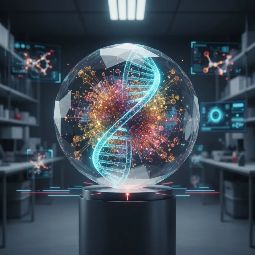
DNA and silicon memory storage represents a fundamental shift in how the technology industry approaches the data storage crisis. Researchers have successfully fused synthetic DNA with crystalline perovskite semiconductors to create a bio-hybrid memory device that performs like existing storage systems while consuming only one-tenth the power. The breakthrough, published in Advanced Functional Materials with a patent application filed, addresses a critical bottleneck: traditional silicon-based storage is approaching its scaling limits as global data generation accelerates.
Key Takeaways
- Synthetic DNA stores 215 million gigabytes of data per gram, nature’s densest storage mechanism.
- Bio-hybrid device uses 10 times less power than current perovskite-based memory systems.
- Stable performance maintained at room temperature for over six weeks and up to nearly 250 degrees Fahrenheit.
- Penn State researchers led the project with funding from NSF’s SemiSynBio program.
- Patent application filed; technology bridges biology and electronics for low-power memory design.
How DNA and silicon memory storage solves the power crisis
Data centers consume staggering amounts of electricity. The bio-hybrid approach tackles this by leveraging DNA’s natural information density—215 million gigabytes per gram—combined with perovskite semiconductors’ electronic properties. Kavya S. Keremane, a postdoctoral researcher in materials science and engineering at Penn State and co-corresponding author of the research, explained the innovation: “Biology and electronics are different domains. Bridging these two fields required developing an entirely new materials platform that allows them to function smoothly together. By combining the information storage capabilities of DNA with the exceptional electronic properties of perovskite semiconductors, we created a bio-hybrid system that fundamentally changes how low-power memory devices can be designed”.
The device’s power efficiency matters enormously. As artificial intelligence workloads expand and data volumes explode, energy consumption has become a limiting factor for cloud infrastructure. A system that delivers identical memory performance while drawing one-tenth the power could reshape data center economics globally. The bio-hybrid prototype maintains stable operation across a wide temperature range—from room temperature for over six weeks to nearly 250 degrees Fahrenheit—outperforming current perovskite-based devices in both thermal stability and power consumption.
Why DNA and silicon memory storage beats current alternatives
Traditional silicon storage has dominated for decades, but it faces fundamental physical limits. Perovskite-based memory systems offer a potential alternative but suffer from higher power consumption and thermal instability compared to the bio-hybrid approach. The synthetic DNA component uses chemically engineered short genetic sequences—commercially available materials—rather than biological DNA extracted from living organisms, making the system practical for manufacturing.

Hao Yan, a Regents Professor at Arizona State University, framed the broader implications: “For decades, information technology has relied almost entirely on silicon. What we’re showing here is that biological molecules, specifically DNA, can be engineered to store and protect information in fundamentally new ways. By treating DNA as an information platform rather than just a genetic material, we can begin to rethink how data is stored, read and secured at the nanoscale”. This perspective reveals why the breakthrough matters beyond engineering specs—it represents a conceptual shift from viewing DNA as a biological curiosity to recognizing it as an engineered material platform.
The technical architecture behind DNA and silicon memory storage
The device integrates two distinct material systems. Synthetic DNA provides the storage density and information capacity. Crystalline perovskite—a semiconductor material already used in solar cells, lasers, and experimental data storage—provides the electronic interface, allowing the system to read and write data using conventional semiconductor techniques. This hybrid approach sidesteps the challenge of interfacing biological molecules directly with silicon electronics; instead, perovskite acts as a translator between biology and conventional electronics.


The research was funded in part by the National Science Foundation’s Semiconductor Synthetic Biology Circuits and Communications for Information Storage (SemiSynBio) program, reflecting growing institutional recognition that biological and electronic approaches may need to merge to overcome silicon’s limitations. Related work at Arizona State University explores DNA nanostructures for ultra-dense data storage with electronic-style readout, suggesting multiple research teams are converging on similar solutions from different angles.
What remains unproven about DNA and silicon memory storage
The current work demonstrates a laboratory prototype with promising performance characteristics. Long-term scalability beyond the prototype stage remains unverified. Manufacturing challenges—how to produce bio-hybrid memory at scale, maintain consistent quality, and integrate it with existing data center infrastructure—have not been addressed in the published research. The device must also prove itself in extended real-world testing beyond the six-week room-temperature stability window documented so far.
Other approaches to next-generation storage exist but follow different paths. Researchers at the University of Southampton have created 5D memory crystals capable of storing the human genome in silica nanostructures with a theoretical lifespan of billions of years and capacity up to 360 terabytes, but this approach does not integrate DNA with semiconductors and uses different physical principles. Chimeric DNA systems under development by NSF-funded projects expand DNA’s coding capacity from four symbols to over twenty by using chemically modified nucleotides, offering another route to higher storage density. The DNA and silicon memory storage approach differs by focusing on integrating DNA with existing semiconductor technology rather than replacing silicon entirely.
Why this matters for data centers and AI infrastructure
The explosion of artificial intelligence training and inference workloads has created unprecedented data storage demands. A memory system that delivers equivalent capacity and speed while consuming one-tenth the power would reduce operational costs and carbon footprint significantly. The thermal stability—maintaining performance from room temperature to nearly 250 degrees Fahrenheit—could also simplify cooling requirements in data center designs, further reducing energy overhead.


The research team’s focus on low-power design reflects a hard constraint facing the industry: electricity consumption limits scalability more than raw materials or manufacturing capacity. DNA and silicon memory storage directly addresses this bottleneck by borrowing nature’s most efficient information storage mechanism and coupling it with proven semiconductor engineering.
What happens next for DNA and silicon memory storage?
The patent application signals the researchers’ intent to commercialize the technology, though timelines for prototype-to-product transitions in materials science typically span years. The next phase would involve scaling from laboratory samples to manufacturable quantities, testing reliability over extended periods, and developing integration pathways with existing storage systems. Collaboration between Penn State’s materials science expertise and Arizona State’s DNA nanotechnology work suggests the research community is building momentum around bio-hybrid approaches.
Could DNA and silicon memory storage replace all current storage?
Unlikely in the near term. The technology excels at low-power, high-capacity static storage—ideal for data centers and archival. Consumer devices requiring fast random access, frequent rewrites, or extreme durability may continue using conventional flash or magnetic storage. The breakthrough’s real value lies in carving out a niche where power efficiency and density matter most: cloud infrastructure, AI training data repositories, and long-term archival systems.
How long until DNA and silicon memory storage reaches the market?
The research is at the patent stage with a working prototype, placing it several years ahead of commercial deployment. Materials science breakthroughs typically require 5-10 years from publication to market introduction, assuming funding continues and manufacturing challenges resolve favorably. Early adopters in data center operations may see pilot deployments within 3-5 years if development accelerates, but mainstream availability is likely a decade away.
The fusion of DNA and silicon memory storage represents the kind of fundamental innovation the technology industry needs as silicon scaling falters and energy constraints tighten. By treating DNA as an engineered material rather than a biological oddity, researchers have opened a new design space for information storage. Whether this specific approach becomes the dominant technology or merely one solution among several, the conceptual shift—that biology and electronics can be merged at the materials level—will reshape how engineers approach future storage challenges.
Edited by the All Things Geek team.
Source: TechRadar


