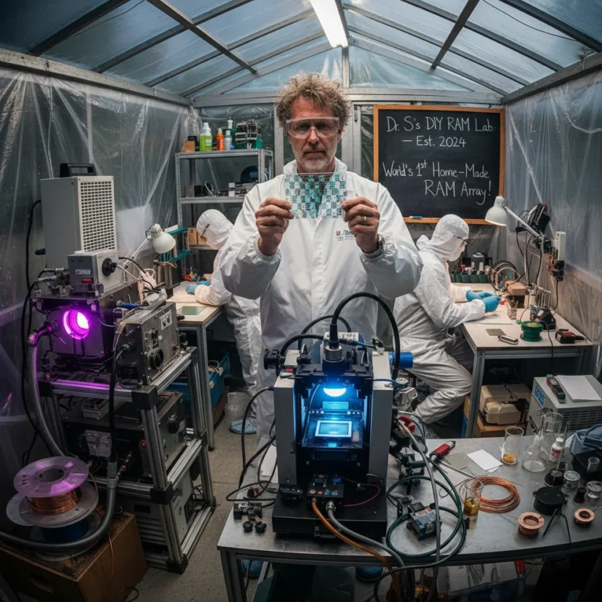
Home-made RAM fabrication just crossed from theoretical hobby into functional reality. Dr. Semiconductor, a YouTuber and semiconductor enthusiast, has successfully fabricated a working array of RAM memory cells with 12pF capacitance inside a Class 100 cleanroom built within his garden shed, marking what he claims is the first time RAM has been produced at home.
Key Takeaways
- Dr. Semiconductor built a Class 100 (ISO 5) cleanroom inside a garden shed with HEPA filtration and positive pressure airflow.
- The shed cleanroom includes plasma etcher, vacuum furnace, custom-software lithography machine, and thin film deposition system.
- Successfully fabricated functional RAM memory cells with 12pF capacitance, claimed as first home-made RAM.
- Cleanroom features dedicated electrical, mini-split climate control, flame-resistant drywall, and water-based epoxy coating.
- Project serves as groundwork for a much larger future RAM array.
From Garden Storage to Semiconductor Lab
Transforming a backyard shed into a semiconductor fabrication facility required methodical planning and engineering discipline. Dr. Semiconductor started with an empty garden shed—no clean air control, no temperature regulation, just wood and space—and systematically converted it into what he describes as a fully functioning semiconductor R&D space. The shed was divided into two distinct zones: a gowning room for transitional entry and the main cleanroom chamber. This separation prevents direct contamination pathways that would compromise the fabrication environment.
The structural foundation relies on flame-resistant drywall instead of expensive plastic paneling, coated with water-based epoxy to create smooth, particle-free, cleanable surfaces. HEPA filtration with positive pressure pushes clean air inward while blocking external contaminants. A dedicated mini-split air conditioning system maintains constant temperature, essential for semiconductor work where thermal fluctuations cause dimensional drift in nanoscale features. Every design choice reflects the reality that cleanroom construction is only one part of an incredibly expensive and complex process.
Custom Tools Drive Home-Made RAM Fabrication
The equipment inside the shed cleanroom reads like an industrial fab condensed into garage dimensions. Dr. Semiconductor equipped the space with a plasma etcher for nanoscale film removal, a vacuum furnace for high-temperature sample annealing, and a custom-built lithography machine constructed from a modified microscope and autonomous software for submicron patterning. He also installed a fume hood for chemical processing, a 3D-printed spin coater for thin film application, an automated robot arm for sample cleaning, and a thin film deposition system for atomic layer building. This combination of commercial equipment, modified tools, and custom fabrication solutions demonstrates that home-made RAM fabrication does not require purchasing a complete industrial system—it requires understanding what each step accomplishes and adapting available resources to achieve it.


The lithography machine exemplifies this resourcefulness. Rather than purchasing a commercial stepper costing hundreds of thousands, Dr. Semiconductor built his own from a microscope, adding custom software that operates it autonomously. This approach compresses the cost and complexity barrier while maintaining the precision required for semiconductor patterning. The plasma etcher removes films at nanoscale dimensions—a capability that separates semiconductor fabrication from merely handling components.
The RAM Achievement and Future Scale
The functional 12pF capacitance RAM array represents proof of concept, not mass production. Capacitance in DRAM cells is measured in picofarads; 12pF is a measurable, functional value that confirms the memory cells store charge and respond to read/write cycles. Dr. Semiconductor’s video “Making RAM at Home” has accumulated 329K views, signaling genuine audience interest in DIY semiconductor work. However, he frames this initial array as groundwork for a much larger future project, indicating he recognizes the distinction between demonstrating feasibility and achieving practical scale.


Prior DIY semiconductor efforts focused on building cleanrooms themselves—an accomplishment, but one that stops short of actual device fabrication. Home-made RAM fabrication advances beyond that milestone by producing functional semiconductor devices, not just the environment to house them. This distinction matters because it proves the entire pipeline—from material preparation through lithography, etching, deposition, and testing—can operate outside industrial fabs, even if at much smaller scale.
Why Home Semiconductor Fabrication Still Matters
Industrial semiconductor fabs cost billions and require teams of specialists. The notion that one person in a shed can produce working RAM cells challenges the assumption that advanced chip manufacturing is exclusively industrial territory. This does not mean home fabs will replace Intel or TSMC—the economics and scale are incomparable—but it does mean the knowledge, tools, and techniques are becoming accessible enough that motivated individuals can experiment with semiconductor physics and fabrication at functional levels.
Dr. Semiconductor’s achievement also highlights how 3D printing, open-source software, and modular equipment have lowered barriers to entry. The spin coater is 3D-printed; the lithography machine runs custom software; the cleanroom uses standard HVAC components and epoxy coating rather than proprietary systems. Each substitution reduces cost while maintaining function. For hobbyists, educators, and researchers in regions without access to shared fab facilities, this model offers a pathway to hands-on semiconductor experience that was previously unavailable outside academic or industrial settings.
Is home-made RAM fabrication practical for others?
Home-made RAM fabrication requires significant capital investment, technical expertise, and space. A Class 100 cleanroom alone demands dedicated HVAC, electrical infrastructure, and material costs. The equipment—plasma etcher, vacuum furnace, lithography system—represents additional substantial expense. Dr. Semiconductor’s success reflects years of semiconductor knowledge and engineering problem-solving. Replicating his setup is feasible for determined enthusiasts but impractical as a cost-effective alternative to purchasing commercial RAM.


What is the next step for this home-made RAM project?
Dr. Semiconductor has indicated the 12pF array is groundwork for a much larger future array. Scaling up means increasing the number of memory cells, improving yield (the percentage of functional cells), and potentially demonstrating more complex memory architectures. The next phase likely involves optimizing his fabrication processes to reduce defects and increase cell density, moving from proof-of-concept toward something approaching practical utility.
Home-made RAM fabrication remains a niche pursuit, but Dr. Semiconductor has demonstrated it is no longer theoretical. The garden shed cleanroom, equipped with custom and adapted tools, produced functional semiconductor devices. Whether others follow this path depends on motivation and resources, but the barrier to entry has shifted from “impossible” to “extremely difficult but achievable.” That shift, however incremental, reshapes what enthusiasts believe is possible in their own backyards.
Edited by the All Things Geek team.
Source: Tom's Hardware